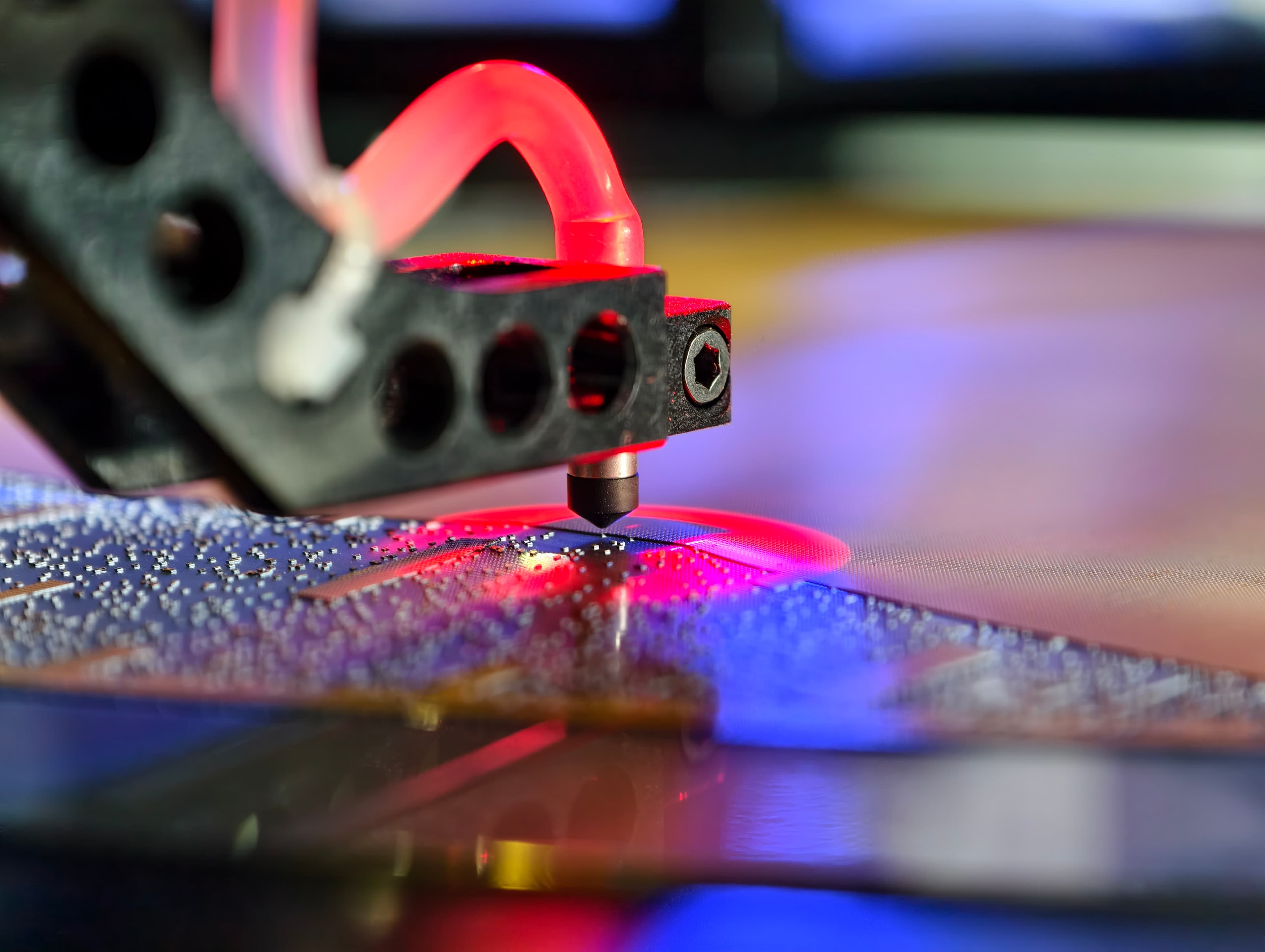
제조

Nextwaves 인레이 칩 본딩 시설

대규모로 고성능 RFID 인레이를 제공하는 최첨단 제조 시설.

팀과 상담하기

연간 생산 능력

짧은 리드 타임으로 대규모 글로벌 주문을 처리할 수 있는 고속 본딩 라인.

1억+

1억+

연간 생산 능력

짧은 리드 타임으로 대규모 글로벌 주문을 처리할 수 있는 고속 본딩 라인.
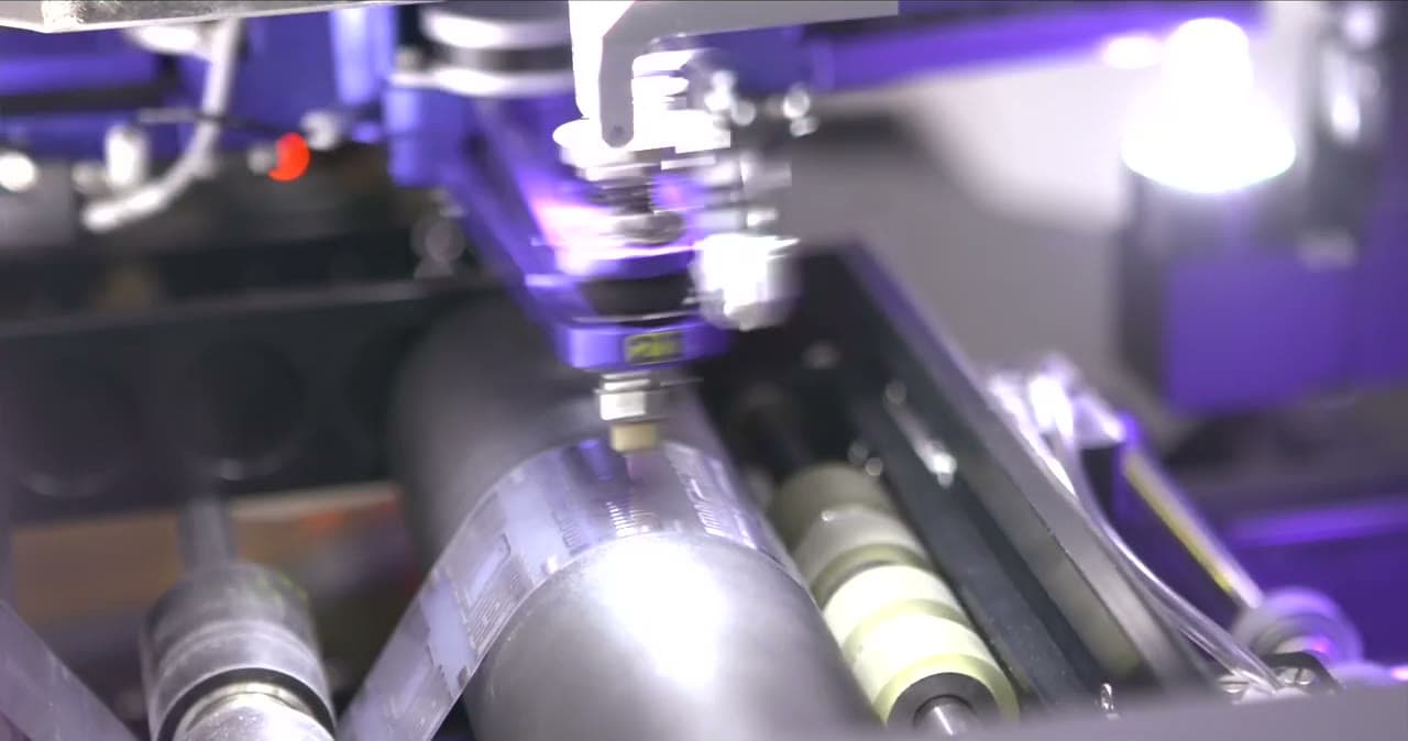
±10µm

본딩 정확도

최대 RF 성능을 위해 완벽한 안테나-칩 연결을 보장하는 첨단 플립 칩 기술.

99.9%

수율

모든 단계에서 자동 광학 검사(AOI) 및 RF 테스트를 통해 결함 없는 납품을 보장합니다.

From design to inlay reel

From the engineering bench to the bonding line, all in Ho Chi Minh City.

  1. 01

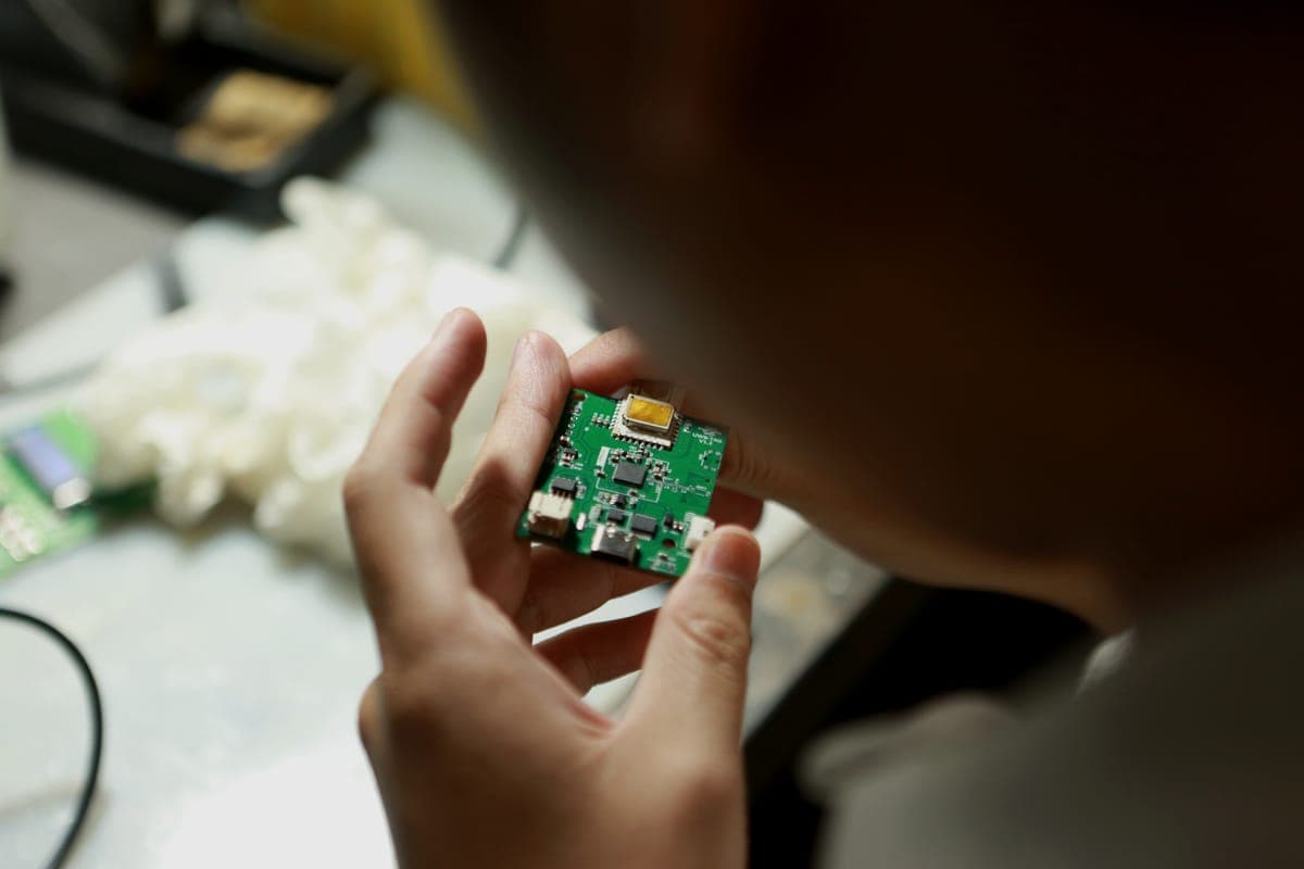
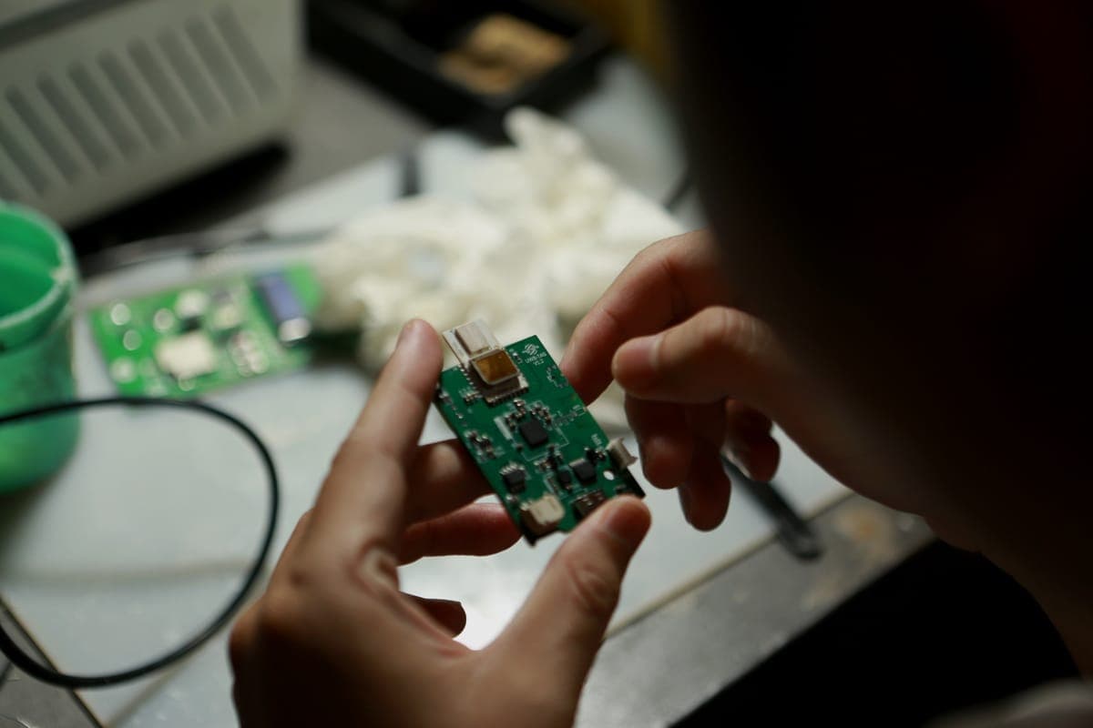
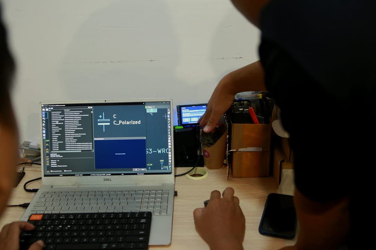
    Hardware design

    Our engineers draw the schematics in KiCad, pick the parts and test every prototype board at the bench before it goes to production.

    4 photos
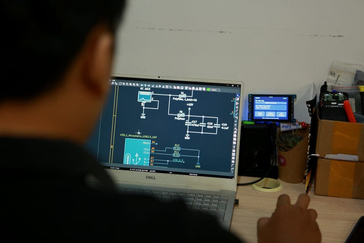
    Drawing the power and USB-C schematic in KiCad
    Inspecting a freshly assembled UWB tag board
    Testing a prototype board at the bench
    Picking parts for the schematic
  2. 02

    Die pick-up

    The diced wafer holds thousands of RFID dies. A vacuum nozzle picks them one at a time under a locating light, ready for bonding.

    5 photos
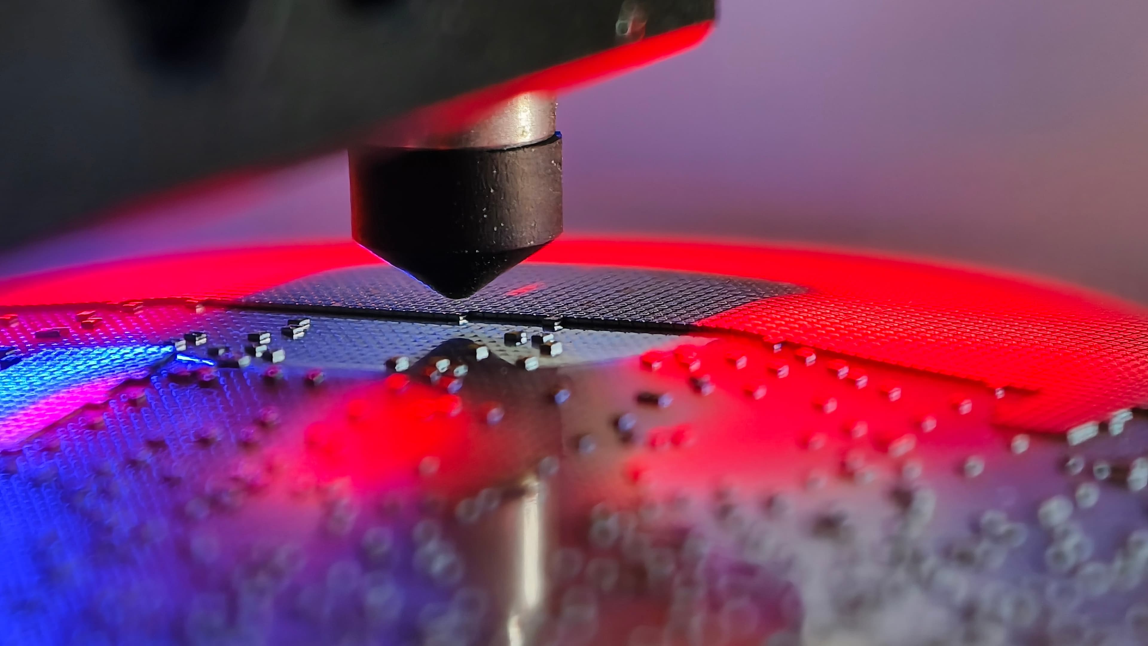
    The pick-up nozzle lowering onto the wafer
    A diced wafer, its dies waiting on the tape
    Picking dies under the locating light
    RFID dies up close
    The pick-up head and its vacuum line
  3. 03

    Flip-chip bonding

    The bond head flips each die and sets it on the antenna's contact pads to within ±10µm.

    2 photos

    The bond tip setting a chip on the antenna pads
    Bonding along the antenna web
  4. 04

    Thermocompression curing

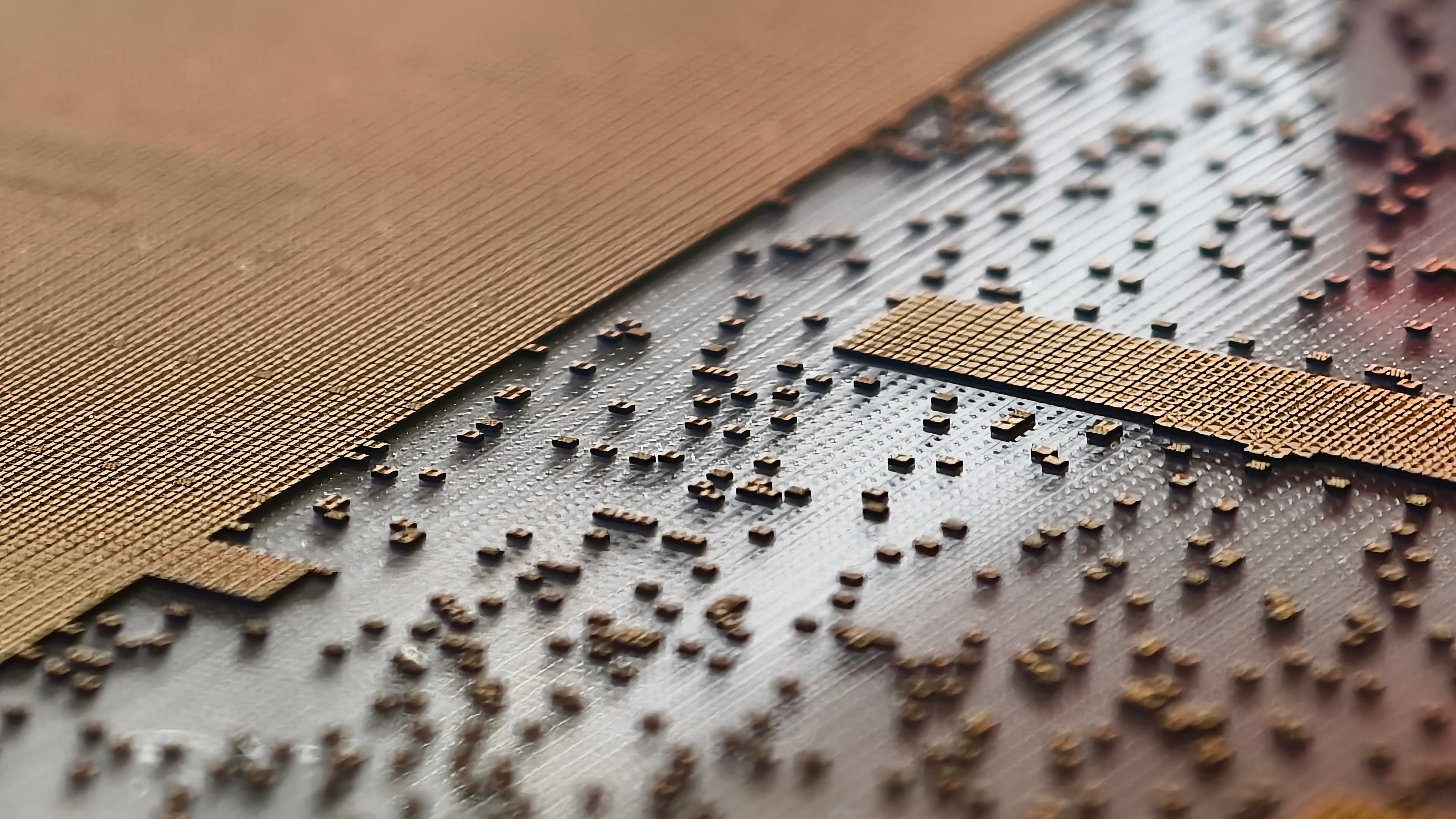
    A row of thermode heads runs along the antenna web, curing the adhesive so every chip stays bonded with a stable contact.

    2 photos
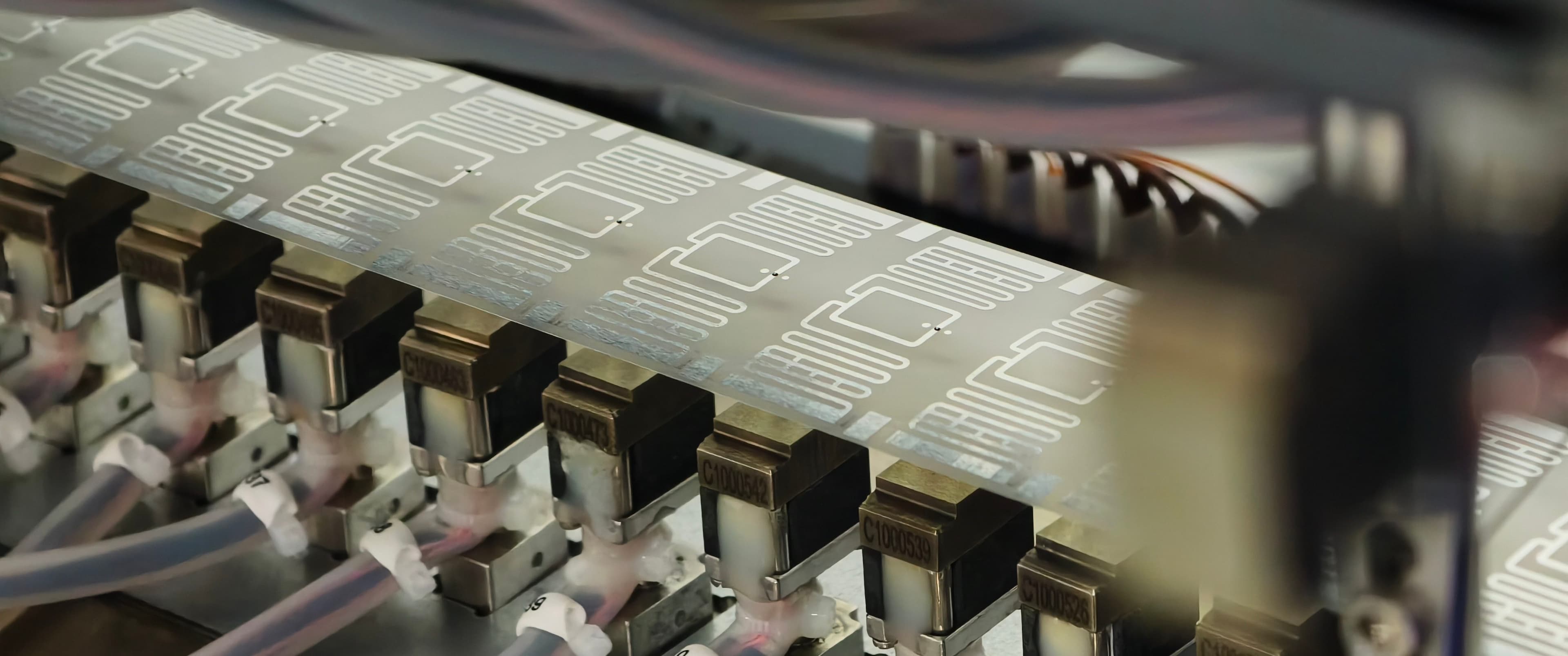
    The row of thermode heads under the web
    The antenna web running through the curing station
  5. 05

    Inspection and rewind

    Every inlay goes through optical and RF checks before the web is rewound into finished reels for delivery.

    2 photos

    Checking antennas and chip placement under light
    Finished inlays running over the rewind roller

태그가 생산되는 시설을 직접 확인하세요

필요한 수량과 일정을 알려주세요. 당사의 본딩 라인이 대규모 생산을 어떻게 처리하는지 보여드리겠습니다.